Connectors and wiring
Every connector on the controller board, what it does, its pin-out and how to wire it. Pin numbers follow the board silkscreen; pin 1 is GND on almost every connector.
RF safety
High RF power. Never operate without a proper load or antenna connected.
Two footprints per connector
Most connectors appear twice on the board under two reference numbers, for example J3 / J4. The first is a JST PH (2.0 mm) side-entry socket, the second is a row of solder pads wired in parallel. Use whichever suits your build: a crimped JST PH lead, or wires soldered straight to the pads. Never use both at once.
Overview
The four diagrams below show the whole system. The sections after them cover each connector in detail.
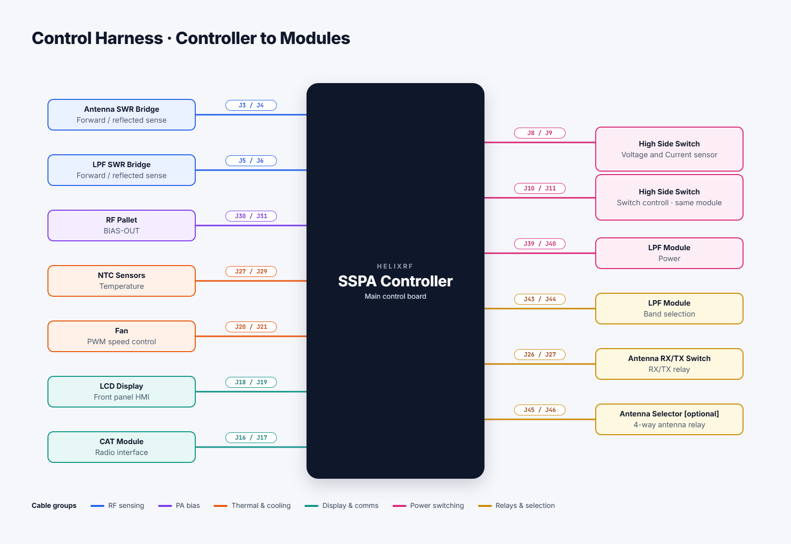
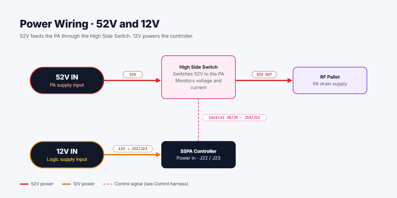
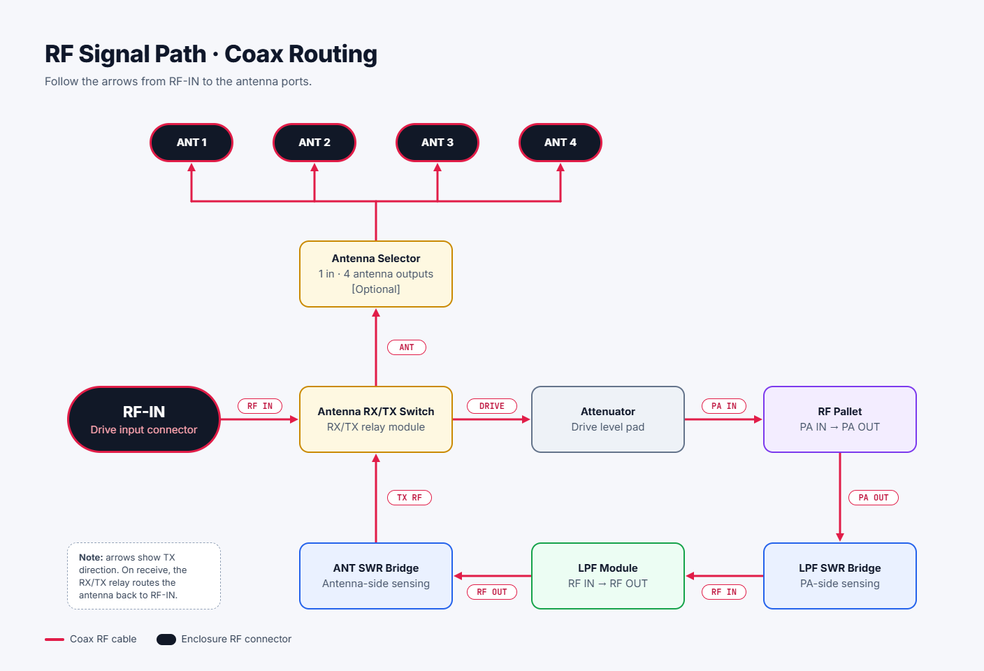
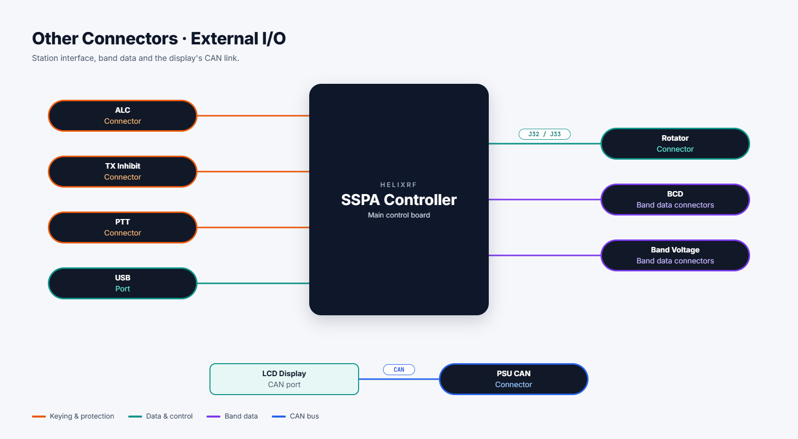
Connector index
| Connector | Name on board | Connects to | Section |
|---|---|---|---|
| J22 / J23 | 12V | 12 V logic supply | Power in |
| J39 / J40 | LPF PWR | LPF module supply | LPF power |
| J8 / J9 | PSU-MON | High Side Switch, voltage and current sense | PSU monitor |
| J10 / J11 | PSU-PROT | High Side Switch, on/off control | PSU protection |
| J30 / J31 | BIAS | RF pallet bias | PA bias |
| J3 / J4 | ANT SWR | Antenna-side SWR bridge | SWR bridges |
| J5 / J6 | LPF SWR | PA-side (LPF) SWR bridge | SWR bridges |
| J28 / J29 | NTC | Two temperature sensors | Temperature |
| J20 / J21 | FAN | Cooling fan | Fan |
| J41 / J42, J43 / J44 | ~LPF, LPF | LPF band relays | LPF band select |
| J45 / J46 | ANT | Antenna selector relays | Antenna selector |
| J26 / J27 | PTT | Radio PTT in, RX/TX relay out | PTT and RX/TX relay |
| J24 / J25 | ALC | Radio ALC and TX inhibit | ALC and TX inhibit |
| J1 / J2 | BAND SELECT | Radio band data, RF sense | Band data |
| J16 / J17 | CAT | CAT / CI-V module | CAT |
| J18 / J19 | 3V3 UART1 | Touch display | Display |
| J32 / J33 | ROT | Antenna rotator | Rotator |
| J34 | USB-C | PC (service) | USB |
| J14 / J15 | FREQ-CNT | Frequency counter / drive protection | Expansion |
| J12 / J13 | I2C | Expansion | Expansion |
| J35 / J36 | NEURAL | Expansion UART | Expansion |
| J37 / J38 | OTA | Firmware update lines | Expansion |
| J7 | SWD | Programmer / debugger | Expansion |
Power
J22 / J23 · 12 V power in
The 12 V logic supply for the controller, the display, the fan and all relay outputs. It is fused on the board (F1, resettable).
| Pin | Signal | Direction | Notes |
|---|---|---|---|
| 1 | GND | ||
| 2 | +12 V | In | [TODO: input range and current needed with all relays on] |
 12 V supply                       Controller J22
 ┌─────────┐                       ┌──────────┐
 │    +12V ├───────────────────────┤ 2  +12V  │
 │     GND ├───────────────────────┤ 1  GND   │
 └─────────┘                       └──────────┘
Warning
The 52 V PA supply never goes to the controller board. It runs through the High Side Switch module (see Power diagram).
J39 / J40 · LPF module power
Supplies 12 V to the LPF relay board. Two pins per rail share the current.
| Pin | Signal | Direction |
|---|---|---|
| 1, 2 | GND | |
| 3, 4 | +12 V | Out |
 Controller J39                     LPF module
 ┌──────────┐                      ┌──────────┐
 │ 3,4 +12V ├──────────────────────┤ +12V     │
 │ 1,2 GND  ├──────────────────────┤ GND      │
 └──────────┘                      └──────────┘
J8 / J9 · PSU monitor
Voltage and current readings from the High Side Switch module, shown on the display and used by the protection. Pin 4 powers the sensor.
| Pin | Signal | Direction | Notes |
|---|---|---|---|
| 1 | GND | ||
| 2 | V_SENSE | In | PA supply voltage, scaled by the module |
| 3 | I_SENSE | In | PA current: shunt amplifier, Hall sensor or BTS current-sense output |
| 4 | +3.3 V | Out | Supply for the sensor |
The sensor type (shunt, Hall or BTS) and its values are set on the display. See Setup and calibration.
 Controller J8                      High Side Switch (sense)
 ┌───────────────┐                 ┌─────────────────┐
 │ 4  +3.3V      ├─────────────────┤ sensor supply   │
 │ 3  I_SENSE    │◄────────────────┤ current out     │
 │ 2  V_SENSE    │◄────────────────┤ voltage out     │
 │ 1  GND        ├─────────────────┤ GND             │
 └───────────────┘                 └─────────────────┘
J10 / J11 · PSU protection
Turns the 52 V PA supply off when the hardware protection latches a fault. Both polarities are provided, so the switch module can use whichever its gate driver needs.
| Pin | Signal | Direction | Notes |
|---|---|---|---|
| 1 | GND | ||
| 2 | ~PROT-VCC | Out | Fault output, inverted sense |
| 3 | PROT-VCC | Out | Fault output |
| 4 | +3.3 V | Out | Supply for the switch logic |
[TODO: state the active level of each pin (switched to GND on fault?) and which one the HelixRF High Side Switch uses.]
 Controller J10                     High Side Switch (control)
 ┌───────────────┐                 ┌─────────────────┐
 │ 4  +3.3V      ├─────────────────┤ logic supply    │
 │ 3  PROT-VCC   ├────────────────►│ enable / kill   │
 │ 2  ~PROT-VCC  ├────────────────►│ (use one)       │
 │ 1  GND        ├─────────────────┤ GND             │
 └───────────────┘                 └─────────────────┘
PA
J30 / J31 · PA bias
Switches the pallet's gate bias. The controller applies bias only while transmitting, after the RX/TX relay has settled (20 ms), and removes it before the relay returns to receive. A protection fault removes it at once.
| Pin | Signal | Direction | Notes |
|---|---|---|---|
| 1 | GND | ||
| 2 | BIAS-IN | In | Bias supply from the pallet |
| 3 | BIAS-OUT | Out | Switched bias back to the pallet's gate-bias input |
| 4 | Gate kill (optional) | Out | Pulls the gate to GND on a fault |
| 5 | +12 V | Out | Supply for an external pinch-off circuit |
| 6 | −12 V | Out | Supply for an external pinch-off circuit |
| 7 | PINCH | Out | Protection-latch signal for a pinch-off circuit |
| 8 | BIAS_CTRL | Out | Logic high while transmitting, for pallets with a bias-enable input |
Most LDMOS pallets need only pins 1–3. Pins 4–8 are for pallets that need a hard gate kill, a negative pinch-off voltage or a separate bias-enable signal. [TODO: wiring notes for the pallets you support.]
 Controller J30                     RF pallet
 ┌───────────────┐                 ┌──────────────────┐
 │ 2  BIAS-IN    │◄────────────────┤ bias supply out  │
 │ 3  BIAS-OUT   ├────────────────►│ gate bias in     │
 │ 4  Gate kill  ├ ─ ─ ─ ─ ─ ─ ─ ─►│ gate (optional)  │
 │ 8  BIAS_CTRL  ├ ─ ─ ─ ─ ─ ─ ─ ─►│ bias enable (opt)│
 │ 1  GND        ├─────────────────┤ GND              │
 └───────────────┘                 └──────────────────┘
       ─── required    ─ ─ optional
RF sensing and thermal
J3 / J4 and J5 / J6 · SWR bridges
DC outputs from the two directional couplers. J3 / J4 reads the bridge on the antenna side (after the LPF). J5 / J6 reads the bridge between the PA and the LPF, which catches a wrong or failed filter. Both feed the power meter and the hardware SWR trip.
| Pin | Signal | Direction | Notes |
|---|---|---|---|
| 1 | GND | ||
| 2 | Reflected (ANT-R / LPF-R) | In | DC from the reflected detector |
| 3 | GND | ||
| 4 | Forward (ANT-F / LPF-F) | In | DC from the forward detector |
Use shielded cable or a twisted pair per signal, and keep it away from the PA output coax.
 SWR bridge                         Controller J3 (antenna) / J5 (LPF)
 ┌──────────────┐                  ┌──────────────┐
 │ FWD detector ├─────────────────►│ 4  FWD       │
 │          GND ├──────────────────┤ 3  GND       │
 │ REF detector ├─────────────────►│ 2  REF       │
 │          GND ├──────────────────┤ 1  GND       │
 └──────────────┘                  └──────────────┘
Calibrate both bridges after wiring; see Power calibration.
J28 / J29 · NTC temperature sensors
Two NTC thermistors, for example one on the pallet heatsink and one on the LPF or the PSU. The fan speed and the over-temperature trip follow whichever reads higher. Each NTC sits between +3.3 V and its sense pin; the board has a 10 kΩ resistor from each sense pin to GND.
| Pin | Signal | Direction | Notes |
|---|---|---|---|
| 1 | +3.3 V | Out | NTC 1 supply |
| 2 | NTC-1 | In | NTC 1 sense |
| 3 | +3.3 V | Out | NTC 2 supply |
| 4 | NTC-2 | In | NTC 2 sense |
Use 10 kΩ NTCs [TODO: confirm recommended NTC value and beta]. Enter each NTC's resistance and beta on the display.
 Controller J28
 ┌──────────────┐        NTC 1 (heatsink)
 │ 1  +3.3V     ├────────/\/\/\────┐
 │ 2  NTC-1     ├──────────────────┘
 │              │        NTC 2
 │ 3  +3.3V     ├────────/\/\/\────┐
 │ 4  NTC-2     ├──────────────────┘
 └──────────────┘
J20 / J21 · Fan
Variable fan speed. The speed ramps from 10 % at the "fan low" temperature to 100 % at "fan high"; the fan never stops completely. Two-wire fans are switched on their negative lead; four-wire PC fans take the PWM signal.
| Pin | Signal | Direction | Notes |
|---|---|---|---|
| 1 | GND | ||
| 2 | PWM | Out | PWM control for 4-wire fans |
| 3 | FAN − | Out | Switched negative for 2-wire fans |
| 4 | +12 V | Out | Fan supply (filtered) |
 Controller J20                 Fan
 ┌──────────────┐              ┌──────────┐
 │ 4  +12V      ├──────────────┤ + (red)  │
 │ 3  FAN −     ├──────────────┤ − (black)│
 └──────────────┘              └──────────┘
 Controller J20                 Fan
 ┌──────────────┐              ┌──────────────┐
 │ 4  +12V      ├──────────────┤ +12V (yellow)│
 │ 1  GND       ├──────────────┤ GND  (black) │
 │ 2  PWM       ├──────────────┤ PWM  (blue)  │
 └──────────────┘              └──────────────┘
   (tach wire not used)
If the fan runs backwards to the temperature (fast when cold), turn on PWM invert on the display.
As above.
[TODO: Rev 4.02 adds GND and raw PWM pins to the fan connector. Add the new pin-out.]
Band and antenna switching
J41 / J42 and J43 / J44 · LPF band select
Eight band outputs to the LPF relay board, one per filter bank. Exactly one output is on at a time. Which bank each band uses is set in the LPF map on the display. The outputs are given twice, so you can use whichever matches your relay board:
- J43 / J44 (LPF): sourcing. The active pin goes to +12 V. Wire each relay coil between the pin and GND.
- J41 / J42 (~LPF): sinking. The active pin goes to GND (open collector). Wire each relay coil between +12 V and the pin.
| Pin | J43 / J44 (sourcing) | J41 / J42 (sinking) |
|---|---|---|
| 1 | BAND1 | ~BAND1 |
| 2 | BAND2 | ~BAND2 |
| 3 | BAND3 | ~BAND3 |
| 4 | BAND4 | ~BAND4 |
| 5 | BAND5 | ~BAND5 |
| 6 | BAND6 | ~BAND6 |
| 7 | BAND7 | ~BAND7 |
| 8 | BAND8 | ~BAND8 |
[TODO: maximum current per output.]
 Controller J43                 LPF module (one bank shown)
 ┌──────────────┐              ┌────────────────────────┐
 │ 1  BAND1     ├─────────────►│ relay coil ──┐         │
 │ …            │              │              GND       │
 │ 8  BAND8     ├─────────────►│ (one per bank)         │
 └──────────────┘              └────────────────────────┘
 Power the LPF board from J39 (+12 V and GND).
 Controller J41                 LPF module (one bank shown)
 ┌──────────────┐              ┌────────────────────────┐
 │ 1  ~BAND1    ├──────────────┤ relay coil ── +12V     │
 │ …            │              │                        │
 │ 8  ~BAND8    ├──────────────┤ (one per bank)         │
 └──────────────┘              └────────────────────────┘
 Relay +12 V comes from J39.
J45 / J46 · Antenna selector
Drives the optional 4-way antenna selector and a separate receive-antenna relay. All outputs are sourcing (+12 V when on). The TX antenna is chosen per band on the display and never changes while transmitting.
| Pin | Signal | Notes |
|---|---|---|
| 1 | ANT1 | TX antenna relay 1 |
| 2 | ANT2 | TX antenna relay 2 |
| 3 | ANT3 | TX antenna relay 3 |
| 4 | ANT4 | Dedicated RX antenna relay |
| 5–8 | EX1–EX4 | Spare outputs [TODO: describe use] |
The TX antenna relays use a cumulative code, so a cascade of three changeover relays selects four antennas:
| Antenna | ANT1 | ANT2 | ANT3 |
|---|---|---|---|
| ANT 1 (default, no relay on) | off | off | off |
| ANT 2 | on | off | off |
| ANT 3 | on | on | off |
| ANT 4 | on | on | on |
 Controller J45                     Antenna selector board
 ┌──────────────┐                  ┌─────────────────────────┐
 │ 1  ANT1      ├─────────────────►│ K1 coil ─┐              │
 │ 2  ANT2      ├─────────────────►│ K2 coil ─┤  coils to    │
 │ 3  ANT3      ├─────────────────►│ K3 coil ─┤  GND         │
 │ 4  ANT4 (RX) ├─────────────────►│ RX relay─┘              │
 └──────────────┘                  └─────────────────────────┘
[TODO: GND and +12 V for the selector board. J45 has no GND pin; take GND from the chassis or J39.]
Radio interface
J26 / J27 · PTT and RX/TX relay
Keying input from the radio and the drive for the RX/TX changeover relay. The controller sequences the relay and the bias so the relay never switches with RF present.
| Pin | Signal | Direction | Notes |
|---|---|---|---|
| 1 | GND | ||
| 2 | ~PTT | In | Active low: radio's TX-GND / SEND output pulls it to GND |
| 3 | nRST-RLY | Out | Switched to GND (open drain) [TODO: describe use] |
| 4 | RX/TX RLY | Out | +12 V while transmitting; flyback diode on board |
 Radio                Controller J26              RX/TX relay
 ┌──────────┐        ┌──────────────┐            ┌──────────┐
 │ SEND/PTT ├───────►│ 2  ~PTT      │            │          │
 │      GND ├────────┤ 1  GND       ├────────────┤ coil −   │
 └──────────┘        │ 4  RX/TX RLY ├───────────►│ coil +   │
                     └──────────────┘            └──────────┘
Test before going on the air
Check that the relay changes over on PTT with no RF applied, before you connect the drive cable.
J24 / J25 · ALC and TX inhibit
ALC feedback to the radio, and a TX-inhibit line that stops the radio from transmitting while a protection fault is latched.
| Pin | Signal | Direction | Notes |
|---|---|---|---|
| 1 | GND | ||
| 2 | ALC (4 V range) | Out | [TODO: confirm range and polarity] |
| 3 | ALC (10 V range) | Out | [TODO: confirm range and polarity] |
| 4 | TX-INH | Out | Switched to GND (open drain) on a fault |
Use the ALC pin that matches your radio's ALC input range.
 Controller J24                     Radio
 ┌──────────────┐                  ┌───────────────┐
 │ 2 or 3  ALC  ├─────────────────►│ ALC in        │
 │ 4  TX-INH    ├─────────────────►│ TX inhibit in │
 │ 1  GND       ├──────────────────┤ GND           │
 └──────────────┘                  └───────────────┘
J1 / J2 · Band data and RF sense
Band information from the radio, by band voltage (Yaesu style), BCD, or an RF sense module. Choose the method and the radio profile on the display. CAT and CI-V use the CAT connector instead.
| Pin | Signal | Direction | Notes |
|---|---|---|---|
| 1 | GND | ||
| 2 | BCD A | In | LSB |
| 3 | BCD B | In | |
| 4 | BCD C | In | |
| 5 | BCD D | In | MSB |
| 6 | BAND-V | In | Band voltage, read up to about 14 V |
| 7 | RF-SENSE | In | From the RF sense module |
| 8 | +5 V | Out | Supply for an RF sense module or band decoder |
 Radio (BAND DATA)              Controller J1
 ┌───────────────┐             ┌──────────────┐
 │ BAND voltage  ├────────────►│ 6  BAND-V    │
 │ GND           ├─────────────┤ 1  GND       │
 └───────────────┘             └──────────────┘
 Radio (BAND DATA)              Controller J1
 ┌───────────────┐             ┌──────────────┐
 │ BAND A        ├────────────►│ 2  BCD A     │
 │ BAND B        ├────────────►│ 3  BCD B     │
 │ BAND C        ├────────────►│ 4  BCD C     │
 │ BAND D        ├────────────►│ 5  BCD D     │
 │ GND           ├─────────────┤ 1  GND       │
 └───────────────┘             └──────────────┘
 RF sense module                Controller J1
 ┌───────────────┐             ┌──────────────┐
 │ +5V in        │◄────────────┤ 8  +5V       │
 │ sense out     ├────────────►│ 7  RF-SENSE  │
 │ GND           ├─────────────┤ 1  GND       │
 └───────────────┘             └──────────────┘
J16 / J17 · CAT / CI-V
Serial link to the radio for automatic band switching by CAT (two-wire serial) or Icom CI-V (single wire). Logic level is 5 V or 3.3 V, set by solder jumper JP2. Pin 4 powers a level converter (RS-232 or USB) if you use one.
| Pin | Signal | Direction | Notes |
|---|---|---|---|
| 1 | GND | ||
| 2 | CAT-RX | In | Data from the radio |
| 3 | CAT-TX | Out | Data to the radio; the CI-V line in CI-V mode [TODO: confirm] |
| 4 | +5 V | Out | Supply for the CAT module |
 Radio / CAT module             Controller J16
 ┌───────────────┐             ┌──────────────┐
 │ TXD           ├────────────►│ 2  CAT-RX    │
 │ RXD           │◄────────────┤ 3  CAT-TX    │
 │ GND           ├─────────────┤ 1  GND       │
 └───────────────┘             └──────────────┘
 Radio (CI-V jack)              Controller J16
 ┌───────────────┐             ┌──────────────┐
 │ tip (CI-V)    ├─────────────┤ 3  CAT-TX    │
 │ sleeve (GND)  ├─────────────┤ 1  GND       │
 └───────────────┘             └──────────────┘
Warning
Most radios' RS-232 ports use ±12 V levels. Do not connect them directly: use a level converter powered from pin 4.
Display and accessories
J18 / J19 · Display
Power and the serial link to the ESP32-P4 touch display. The display also passes firmware updates to the controller over this link.
| Pin | Signal | Direction | Notes |
|---|---|---|---|
| 1 | GND | ||
| 2 | RX | In | 3.3 V UART, from display TX |
| 3 | TX | Out | 3.3 V UART, to display RX |
| 4 | +5 V | Out | Display supply |
 Controller J18                     Display
 ┌──────────────┐                  ┌──────────────┐
 │ 4  +5V       ├─────────────────►│ +5V          │
 │ 3  TX        ├─────────────────►│ RX           │
 │ 2  RX        │◄─────────────────┤ TX           │
 │ 1  GND       ├──────────────────┤ GND          │
 └──────────────┘                  └──────────────┘
The display's own CAN port connects to the PSU CAN connector, where fitted (see the "Other I/O" diagram).
J32 / J33 · Rotator
Antenna rotator control: two relay outputs and the position potentiometer. Supports 360° and 450° rotators with 3-point calibration.
| Pin | Signal (board label) | Direction | Notes |
|---|---|---|---|
| 1 | GND | ||
| 2 | ROT-V | In | Position pot wiper |
| 3 | ROT-L | Out | Relay driver, switched to GND |
| 4 | ROT-R | Out | Relay driver, switched to GND |
[TODO: check rotation direction. In the schematic, pin 3 (ROT-L) is driven by the output the firmware calls CW (ROT-R), and pin 4 by CCW. Confirm on a real rotator and fix the labels.] [TODO: the pot needs a reference voltage from the rotator control box; give the maximum voltage allowed on ROT-V.]
 Controller J32                     Rotator control box
 ┌──────────────┐                  ┌───────────────────────┐
 │ 3  ROT-L     ├──────────────────┤ relay A coil ── +V    │
 │ 4  ROT-R     ├──────────────────┤ relay B coil ── +V    │
 │ 2  ROT-V     │◄─────────────────┤ pot wiper             │
 │ 1  GND       ├──────────────────┤ GND / pot low end     │
 └──────────────┘                  └───────────────────────┘
J34 · USB-C
USB 2.0 device port on the controller. [TODO: what owners use it for (service log, firmware recovery?).]
Expansion and service connectors
These connectors are not needed for a normal build.
| Connector | Name | Pins | Use |
|---|---|---|---|
| J14 / J15 | FREQ-CNT | 1 GND · 2 LVDS+ · 3 LVDS− · 4 PROT-DRIVE (in) | Frequency counter input (LVDS) and an external drive-overload fault input |
| J12 / J13 | I2C | 1 GND · 2 SCL · 3 SDA · 4 +3.3 V | Expansion, on the same bus as the settings EEPROM |
| J35 / J36 | NEURAL | 1 GND · 2 RX · 3 TX · 4 +5 V | Expansion UART (3.3 V) |
| J37 / J38 | OTA | 1 GND · 2 EXT-IO1 · 3 BOOT0 · 4 nRST | Firmware recovery lines [TODO: when this cable is needed] |
| J7 | SWD | 1 +3.3 V · 2 SWDIO · 3 GND · 4 SWCLK · 5 SWO · 6 nRST | STM32 programmer / debugger (2×3, 2.54 mm) |
[TODO: say which of these are reserved for future HelixRF modules.]